Introduction
Theory of Operation
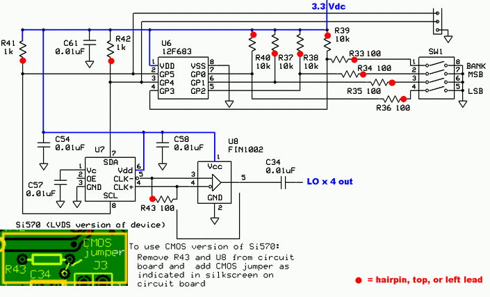
The local oscillator (U7)is a programmable oscillator, whose programmatic parameters
are set by the microcontroller, U6.
U6 is programmed with 16 different values corresponding
to the settings of dip switch SW1. Without U6 in the circuit, U7 would default to
an output frequency of 56.320 mHz. The IC U8 is needed if the version of U7 is the
"LVDS" version. If U7 is a CMOS version, U8 (and R43) is not required and, instead
a jumper wire is installed to bypass them.
This LO stage must produce an output rf signal that is four times the desired center frequency for the radio. This is then fed to the dividers/phasors section to produce the two center-frequency signals that are in quadrature.
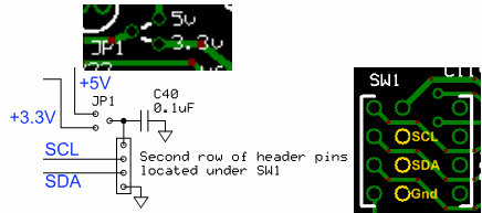
The board has also been designed to include I2C SDA and SCL signal access as well as either regulated 5 volts or 3.3 volts. Under the DIP switch location is a second row of holes such that a double-row header, eight pins in all, may be mounted in place of the DIP switch. The signals available on the header include the four DIP switch inputs to the PIC, GND, SDA, SCL and either regulated 5 volts or regulated 3.3 volts. (The regulated voltage selection is by soldering in a wire jumper at a three hole via the "JP1" group near the DIP switch position.)
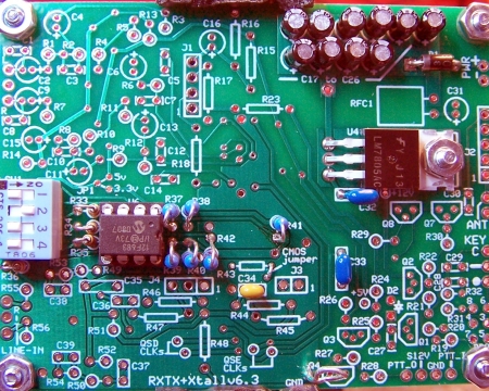
Schematic
Summary Build Notes
- Install U8 (if LVDS), then U7
- Install SW1
- Install Resistors R33-R43 (skip R43 if CMOS)
- Install C34
- Install U6 socket
- Plug in U6
- Test the Stage
Bill of Materials
| Check | Designation | Component | (Color) Code | Type | Qty | Notes |
|---|---|---|---|---|---|---|
| [__] | C34 | 0.01 uF | 103 | ceramic | 1 | |
| [__] | R33 | 100 | brown-black-brown-gold | Resistor 5% 1/6W | 1 | E-W |
| [__] | R34 | 100 | brown-black-brown-gold | Resistor 5% 1/6W | 1 | E-W |
| [__] | R35 | 100 | brown-black-brown-gold | Resistor 5% 1/6W | 1 | E-W |
| [__] | R36 | 100 | brown-black-brown-gold | Resistor 5% 1/6W | 1 | E-W |
| [__] | R37 | 10 k | brown-black-black-red-brown | Resistor 1% | 1 | N-S |
| [__] | R38 | 10 k | brown-black-black-red-brown | Resistor 1% | 1 | N-S |
| [__] | R39 | 10 k | brown-black-black-red-brown | Resistor 1% | 1 | S-N |
| [__] | R40 | 10 k | brown-black-black-red-brown | Resistor 1% | 1 | S-N |
| [__] | R41 | 1 k | brown-black-black-brown-brown | Resistor 1% | 1 | N-S |
| [__] | R42 | 1 k | brown-black-black-brown-brown | Resistor 1% | 1 | S-N |
| [__] | R43 | 100 | brown-black-brown-gold | Resistor 5% 1/6W | 1 | FlatH (Omit for CMOS) |
| [__] | SW1 | 4-pos dip switch | Dip Switch (8 pins) | 1 | mount so pos 1 is toward top of board | |
| [__] | U6 | 12F683 | CPU and socket | 1 | (top) | |
| [__] | U7 | Si570 LVDS or CMOS | Programmable XO/VCXO | 1 | (bottom) | |
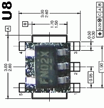
| [__] | U8 | FIN1002 | SOT-23 Diff LVDS Rcvr | 1 | (bottom) Omit for CMOS |
Detailed Build Notes
Bottomside Components
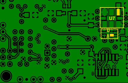
Mount the two ICs (U8, then U7)
. Take ESD precautions. See the guide for mounting SMT ICs.Take great care mounting U8. It is
very tiny and mounts just below pins 4 and 5 of U7. This is an area that is
very ripe for solder bridges!
Carefully check the soldering of U8,
especially around pin 2 (the ground connection) and pin 5 (VCC). You do not want to
short 5Vdc to ground at that point! A good post-soldering test on U8 is to
check the resistance between U8 pin 1 and ground. If it is low, you have a
soldering problem.
Note: if the kit is a CMOS SI570, then do NOT install U8.

| Check | Designation | Component | Picture |
|---|---|---|---|
| U8* (omit if Si570 is CMOS) | FIN1002 |
|
|
|
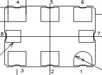
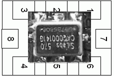
U7
(If there is a "C" at the beginning of the part number just after the Si570 then it is a 3.3 volts CMOS version, otherwise it is an LVDS version) |
Si570 CMOS (or LVDS) |
|
Topside Components
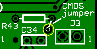
SI570 - CMOS vs. LVDS

If the kit is a CMOS SI570 kit:
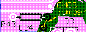
- Do NOT install R43 and U8
- Instead, install a jumper wire between the hole of R43 and the hole connected to U8-Pin5 (reference the illustration above).
- When installing the jumper (if you do), you may want to install it so that you can clip test leads on the jumper.
For a discussion of SI570's versions and the need for the FIN1002, see see the analysis by J. K. DE Marco PY2WM.
Topside Layout
Mount SW1
Mount the 8 pin Dip Switch. Orient the switch such that the numbers (1, 2, 3, 4) are closest to the right hand edge of the board and read, in their ordinal sequence, from top to bottom1.
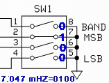
This switch provides a means to select one of 16 "center" frequencies, depending upon the settings for SW1.
1 If you accidentally mount SW1 backwards (as the author did on an earlier project), all is not lost. The switches will still work; you'll just have to remember that the MSB corresponds to switch #4 and the LSB corresponds to #1 when dialing in the frequency "nibbles".
Mount the resistors
first (see the guide to mounting resistors) .If your Si570 is the COMS version, save one of the clipped leads from the 100 ohm resistors to use in the CMOS jumper.
| Check | ||||||
|---|---|---|---|---|---|---|
| Check | Designation | Component | (Color) Code | Type | Qty | Notes |
| [__] | R33 | 100 | brown-black-brown-gold | Resistor 5% 1/6W | 1 | E-W |
| [__] | R34 | 100 | brown-black-brown-gold | Resistor 5% 1/6W | 1 | E-W |
| [__] | R35 | 100 | brown-black-brown-gold | Resistor 5% 1/6W | 1 | E-W |
| [__] | R36 | 100 | brown-black-brown-gold | Resistor 5% 1/6W | 1 | E-W |
| [__] | R37 | 10 k | brown-black-black-red-brown | Resistor 1% | 1 | N-S |
| [__] | R38 | 10 k | brown-black-black-red-brown | Resistor 1% | 1 | N-S |
| [__] | R39 | 10 k | brown-black-black-red-brown | Resistor 1% | 1 | S-N |
| [__] | R40 | 10 k | brown-black-black-red-brown | Resistor 1% | 1 | S-N |
| [__] | R41 | 1 k | brown-black-black-brown-brown | Resistor 1% | 1 | N-S |
| [__] | R42 | 1 k | brown-black-black-brown-brown | Resistor 1% | 1 | S-N |
| [__] | R43 | 100 | brown-black-brown-gold | Resistor 5% 1/6W | 1 | FlatH (Omit for CMOS) Note: watch out if you are installing R43. It is easy to install it to the wrong holes due to the proximity of the CMOS jumper holes! |
Mount C34
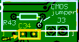
Mount the ceramic capacitor C34 (see guide for mounting ceramic capacitors).
Take care in mounting C34 in the correct holes
(the two horizontally oriented holes just below the holes for R43).
Thanks to David KD0R for identifying the potential for erroneously mounting C34 in the holes
intended for J3
| Check | Designation | Component |
|---|---|---|
| C34 | 0.01 µF (code 103) |
Mount the socket for U6
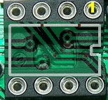
The socket should be oriented so that the notched end is on the right (be careful placing the pins correctly - "measure twice, cut once")
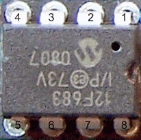
Plug U6 into its socket
Take care to match the notch correctly.| Check | Designation | Component | Picture |
|---|---|---|---|
| U6 |
12F683
(topside)
|
|
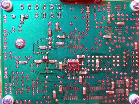
Completed Board
Topside
Bottomside
Testing
Current draw here is for the CMOS version of the Si570. Adjust these appropriately for the LVDS version's higher current draw.
Current Limited Power Test
- Connect a 100 ohm resistor in series with the power line and apply 12 V dc power
- the current should be relatively low (less than 120 mA (around 75 mA is nominal))
- Measure the voltage WRT ground at the +5 V and at the 3.3 Vdc testpoints.
- A voltage of around 2 V dc indicates the power rails are not shorted
Current Draw (DMM )
- If your kit is the LVDS version, expect your readings to be a little higher by about 10 - 15 mA
- Remove the current-limiting resistor. Subsequent tests in this stage are with the current-limiting resistor OUT of the circuit.
- First, you want to measure the current draw with U6 NOT plugged in and the dip switches all in the OFF position. You should a maximum draw of < 84 mA. (Author got 75 mA). Yours: _____________________
- Then, turn all the dip switches ON (U6 still NOT plugged in) and the current draw should be slightly more (1 or 2 mA more). Author measured 76 mA. Yours: _____________________
- Finally, with the power off, reset the dip switches for 7.046 MHz ("0100" as shown in the " as shown in the SW1 Settings), plug in U6, power up, and measure the current draw. This should now be no more than 84 mA. Your measurement is: ___________________________
- You can You can try other switch settings for current draw and the measurements should a swing of about 10 mA, depending upon the SW1 settings from SW1=0000" to SW1="1111".
SSW1/U6 Tests (DMM - 3.3 Vdc, 33 mVdc)
You can test the SW1 programming of U6 by checking the dc voltages at pins 1 thru 7.
Pins 1 thru 3 should always be at the 3.3V rail Vdc.
Voltages at pins 4 thru 7 will vary, depending upon their corresponding dip switch settings (pins 4 thru 7 correspond to dip switches 1 thru 4):.
- When the switch is ON, the corresponding voltage drops to LOW (< 40 mV).
Your measurement is: _____________________ - When the switch is OFF, the corresponding pin's voltage is HIGH (at the 3.3 V
rail).
Your measurement is: _____________________ - If the voltages are not as expected, remove U6 from its socket and retest to ensure that the SW1/U6-Socket wiring is good.
- In this case, if the tests are passed with U6 removed, you should suspect U6.should suspect U6.
- If pins 2 and 3 do NOT measure at the 3.3V rail, investigate the solder connections on U7
Frequency Test
You can validate the LO's frequency output by tuning your HF receiver to four times one of the center frequencies (see SW Settings) and loosely coupling the receiver's antenna via a tickler wire close to the board going to the antenna socket. You should hear the output as quieting in the receiver in AM mode (or a tone if in CW mode).
Some builders have experienced the case where a given switch setting seems to yield signals at 3 times the expected frequency value, only to discover that they were actually getting the third harmonic. (see the series of reflector mesages begining with message #30011).
(Optional) LO Output (Scope/Freq Counter)
Measure the frequency of the signal at the lower CMOS jumper hole. The Local Oscillator should output a signal at the four times the center frequency selected by the switch settings of SW1.
Do not attempt these scope tests unless you have a good quality, calibrated scope with correctly compensated probes. Lesser quality scopes are good for little more than indicating the presence or absence of a signal, something you can do with an external ham radio RX.
Test
- Set the switches of SW1 to 0100 to get a center frequency of 7.046 MHz
- (See Sw1 Switch Settings)
- Apply power to the board
- Test the output of (U8 in the LVDS version of the kit or U7 in the CMOS version)
at the lower of the twoholes provided for the CMOS jumper: the frequency should
about 28.18 MHz (4 times the desired center frequency of 7.046 MHz).
The AC pk-pk voltage should be aproximately equal to or less than 3.3 V p-p
The waveform should approximate a square wave (depending upon the bandwidth and calibration of your scope - see below). - If you get 56.32 MHz (or 14.08 times 4) with SW1 set as above, or regardless of
SW1 settings, this means:
- that U6 has not been installed or
- U6 has been incorrectly installed or
- pins 7 or 8 of U7 may have bad solder joints