Home BOM PS LO DIV Op-Amp RF Mixer Connect
VI – Softrock Lite V6.2 – Mixer
In this stage, we will be adding the signal path up to the point that the signal is coupled to the OPAmps (R14) and to the mixer (R8 and R9)
Parts
|
Designation |
Description |
Type
Component |
Quantity |
|
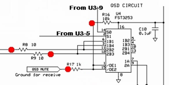
U4 |
FST3253 |
SOIC (SMT) IC |
1 |
|
R8, R9 |
10 Ohm |
¼ W 1% |
2 |
|
R16 |
10 k Ohm |
¼ W 1% |
1 |
|
R17 |
1 k Ohm |
¼ W 1% |
1 |
|
C10 |
0.1 uF |
SMT Cap |
1 |
Schematic
Installation Notes
IC (SMT U4)
Again, the main challenge in this step is the installation of the FST 3253 SMT commutating switch (U4) on the bottom side of the board. This IC is the only 16 pin IC in the kit.
![]() Electro Static
Discharge precautions (e.g., anti-static mat, anti-static wrist-strap, grounded
tip soldering iron) must be taken when handling/installing these ICs See the excellent video tutorials on SMT
soldering at Sparkfun.com and KC0WOX’s video (Surface Mount Soldering
IC's).
Electro Static
Discharge precautions (e.g., anti-static mat, anti-static wrist-strap, grounded
tip soldering iron) must be taken when handling/installing these ICs See the excellent video tutorials on SMT
soldering at Sparkfun.com and KC0WOX’s video (Surface Mount Soldering
IC's).
The ICs in the kit are such that if an IC provided in the kit fits an IC mounting location on the circuit board, then the IC is right for that location.
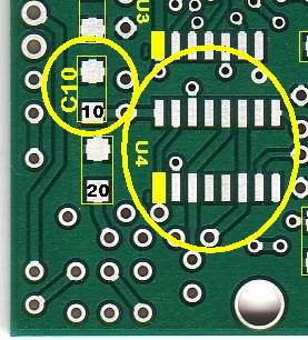
Orient U4 on its pads so that the pin 1 corner of the IC matches the small “1" (it also looks like a “0”) mark in the copper on the bottom side of the board. In general, pin 1 of an SOIC packaged IC is in the lower left corner of the package when the printing on the package top reads upright, from left to right.
Tack-solder one corner pin of U4 and reheat the tacked pin as necessary to line up U4 on its pads properly.
Double-check the orientation of U4 and the line up of the IC on its pads with magnification and good lighting. You do NOT want to install U4 oriented incorrectly. If all is well, carefully solder the rest of the leads to their pads.
Carefully and closely inspect the pins to look for bridges caused by excessive solder or debris on or around the pads. Use solder wick to remove any excess solder or solder bridges between IC pins.
Capacitors
c C10 .01 uF SMT (mount in bottom-side location indicated above
Resistors
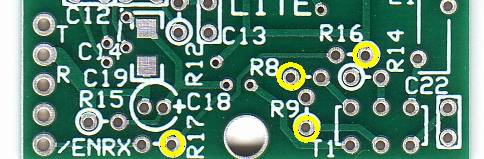
c R8 10 Ohm (east-west)
c R9 10 Ohm (south-north)
c R16 10k Ohm (west-east)
c R17 1k Ohm (west-east)
Tests
Current Draw
The circuit under power should draw approximately 30 mA. Author’s results: 30.8 mA
Resistance Test
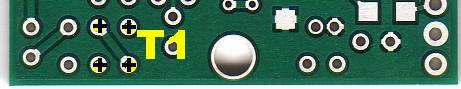
As a further test of your RF Transformer, measure the resistance with respect to ground of the secondary terminals of T1. In each case you should see a resistance of ~790 ohms. Author’s results = 789 ohms.
Voltage Tests (Power On)
Make sure you have enabled the shunt wire between the "/ENRX" terminal and ground, as directed in the Power Supply Stage. If that has not been done, you will get incorrect voltages in the Pin1/Pin15 test and the mixer will not work.
|
T0est
Point |
Expected
Value |
Units |
Author’s
Results |
Measured
Value |
|
U4-1 & 15 (R16 hairpin) |
0.45 |
Vdc |
0.451 |
|
|
U4-2 (S1) |
2.5 |
Vdc |
2.31 |
|
|
U4-3 & 12 |
2.5 |
Vdc |
2.34 |
|
|
U4-6 & 11 |
2.5 |
Vdc |
2.34 |
|
|
U4-7 (1A) |
2.5 |
Vdc |
2.34 |
|
|
U4-8 |
0 (GND) |
Vdc |
0 |
|
|
U4-9 (2A) |
2.5 |
Vdc |
2.34 |
|
|
U4-14 (S0) |
2.5 |
Vdc |
2.29 |
|
|
U4-16 |
5 |
Vdc |
4.94 |
|
1 Initially, this measured out as 4.47 Vdc. The author had reversed R16 and R17, resulting in a 1k-10k voltage divider, instead of the designed 10k-1k divider. The result was that the voltage at pins 1 & 15 was:
4.94 * 10000/(10000+1000)=.9090909 * 4.94 = 4.49 Vdc
instead of
4.94 * 1000/(10000+1000)=.090909+4.94=.45 Vdc
After some messy removal of the reversed resistors and replacement with some junquebox equivalents, the measurement was now within design parameters (see the completed topside picture (notice R17 and R19 are “different” in appearance from the others on the board).
RF Injection
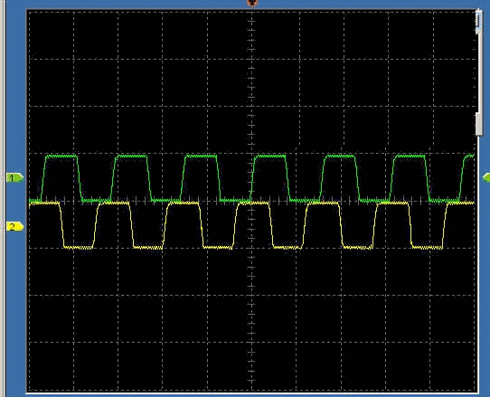
Inject an RF input frequency of 7.040 MHz at 50 mv amplitude. This level makes it easier to look at with a scope and it's not overloading our board. With a center frequency of 7.056 MHz, this should cause a 16 kHz audio frequency at the tip/ring outputs of the board.
Connect a scope’s probes to the ring and to the tip pads on the board and measure the frequency and p-p voltage. With a 50mV p-p input RF signal you should see a 1.6 V p-p output at an audio frequency that is equal to the difference between the RF frequency and the LO Center frequency. The signals at the ring and tip outputs should be 90 degrees out of phase with one another. The image below shows the result of feeding a 50 mV 7/040 MHz signal into the receiver’s antenna terminals.
Alternative to scope: you can connect the ring and tip outputs to your sound card’s stereo inputs, download, install, and run Rocky, and observe the signal on Rocky’s spectrum view.
Completed Stage
Congratulations. You have completed the actual construction of the kit. The only remaining step is to connect the board to the outside world. Once you have done that, you can run Rocky to test its on-the-air performance and, hopefully, move ahead to the installation into the enclosure of your choice. If you do decide to place the radio in, say, an Altoids tin or other metal enclosure, please note that the antenna input must be isolated from circuit and chassis ground.
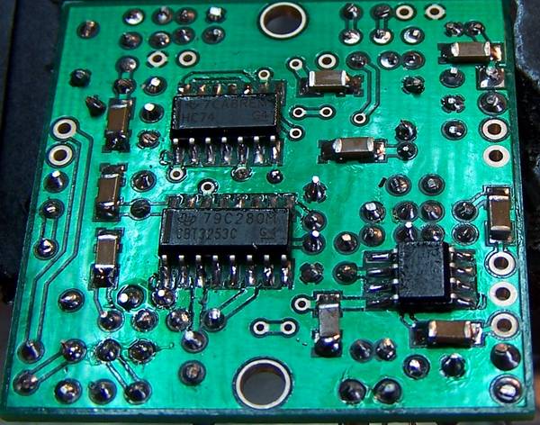
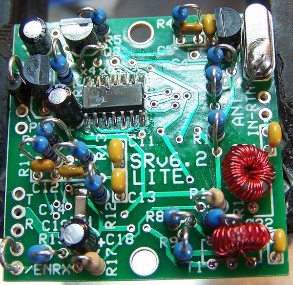
Topside
Bottomside