Home BOM PS LO DIV Op-Amp RF Mixer Connect
III – Softrock Lite V6.2 – Dividers
Parts
|
Designation |
Description |
Type
Component |
Quantity |
|
U2 |
74HC74 |
SOIC-14 (14 pins) |
1 (topside) |
|
U3 |
74HC74 |
SOIC-14 (14 pins) |
1 (bottom side) |
Schematic
Installation Notes
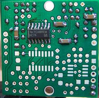
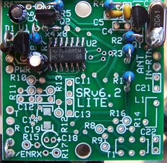
The main challenge in this step is the installation of the two 74HC74 SMT dual flip-flops (U2 and U3). U2 is on the top side and U3 is on the bottom side of the board. These 74HC74 ICs are the only 14 pin ICs in the kit. Electro Static Discharge precautions (e.g., anti-static mat, anti-static wrist-strap, grounded tip soldering iron) must be taken when handling/installing these ICs See the excellent video tutorials on SMT soldering at Sparkfun.com and KC0WOX’s video (Surface Mount Soldering IC's).
The ICs in the kit are such that if an IC provided in the kit fits an IC mounting location on the circuit board, then the IC is right for that location.
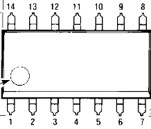
Orient the IC on its pads so that the pin 1 corner of the IC matches the small “1" (it also looks like a “0”) mark in the copper on the bottom side of the board. In general, pin 1 of an SOIC packaged IC is in the lower left corner of the package when the printing on the package top reads upright, from left to right. You may also see a dimple in the corner by pin 1 or a stripe on the pin 1 side (as in the Author’s kit – see completed bottomside picture below).
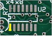
Tack-solder one corner pin of an IC and reheat the tacked pin as necessary to line up the IC on its pads properly. Check the orientation of the IC and the line up of the IC on its pads with magnification and good lighting. If all is well, carefully solder the rest of the leads to their pads.
Carefully and closely inspect the pins to look for bridges caused by excessive solder or debris on or around the pads. Use solder wick to remove any excess solder or solder bridges between IC pins.
c
Mount and solder U2 74HC74 on the 14 pin pad on
the topside of the board (pin 1 is at lower left)
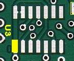
c Mount and solder U3 74HC74 on the 14 pin pad on the bottom side of the board
Tests
Current Draw
c Installing U2 and U3 should increase the current draw from 10.8 mA to 24 mA (Author measured 24.4 mA).
Voltages for U2
|
Pins |
Expected |
(Author’s) |
Yours |
|
1 |
+5 Vdc |
4.92 |
|
|
2 |
+2.5 Vdc |
2.47 |
|
|
3 |
+3.2 Vdc (Q1 collector) |
3.23 |
|
|
4 |
+5 Vdc |
4.92 |
|
|
5 |
+2.5 Vdc |
2.44 |
|
|
6 |
+2.5 Vdc |
2.47 |
|
|
7 |
0 Vdc |
0 |
|
|
8 |
+2.5 Vdc |
2.47 |
|
|
9 |
+2.5 Vdc |
2.43 |
|
|
10 |
+5 Vdc |
4.92 |
|
|
11 |
n/a |
n/a |
n/a |
|
12 |
n/a |
n/a |
n/a |
|
13 |
+5 Vdc |
4.92 |
|
|
14 |
+5 Vdc |
4.92 |
|
Voltages for U3
|
Pins |
Expected |
(Author’s) |
Yours |
|
1 |
+5 Vdc |
4.92 |
|
|
2 |
+2.5 Vdc |
2.47 |
|
|
3 |
+2.5 Vdc |
2.44 |
|
|
4 |
+5 Vdc |
4.92 |
|
|
5 |
+2.5 Vdc |
2.45 |
|
|
6 |
+2.5 Vdc |
2.47 |
|
|
7 |
0 Vdc |
0 |
|
|
8 |
+2.5 Vdc |
2.47 |
|
|
9 |
+2.5 Vdc |
2.44 |
|
|
10 |
+5 Vdc |
4.92 |
|
|
11 |
+2.5 Vdc |
2.47 |
|
|
12 |
+2.5 Vdc |
2.44 |
|
|
13 |
+5 Vdc |
4.92 |
|
|
14 |
+5 Vdc |
4.92 |
|
If these voltages do not reflect the above expected values, there is a strong likelihood that there have been some solder bridges introduced in the installation process. Check and recheck the pins, preferably with strong magnification.
Waveforms
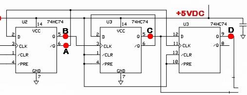
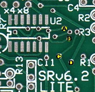
(See testpoints A, B, C, and D in above image)
c A: The /Q output of U2 (pin 6). Should be ½ of the LO frequency, or 14.112 MHz and 180 degrees out of phase with
c B: The Q output of U2 (pin 5). Should be same frequency as pin 5 and 180 degrees out of phase
c C: The Q Output of the first half of U3 (pin 5). The signal amplitude should be between 7.5 and 9 V p-p. The waveform should be the target center frequency (7.056 MHz) and 90 degrees out of phase with
c D: The Q output of the second half of U3 (pin 9). The signal amplitude should be between 7.5 and 9 V p-p. The waveform should be the target center frequency (7.056 MHz) and 90 degrees out of phase with pin 5’s signal.
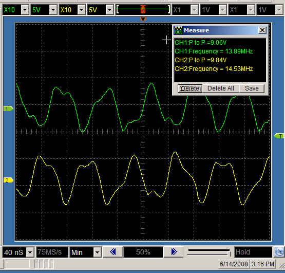
Testpoints A and B – FLO/2
Not: the author’s scope is not the best and struggles with depicting square waves at high frequencies. Thus, the picture below shows, at best, a faint approximation of the square wave output of the first divider stage. Similarly, the frequency readouts are just approximations.
This test shows the LO frequency of 28.224 MHz after the first division, yielding 2 signals of 14.112 MHz and 180 degrees our of phase with each other.
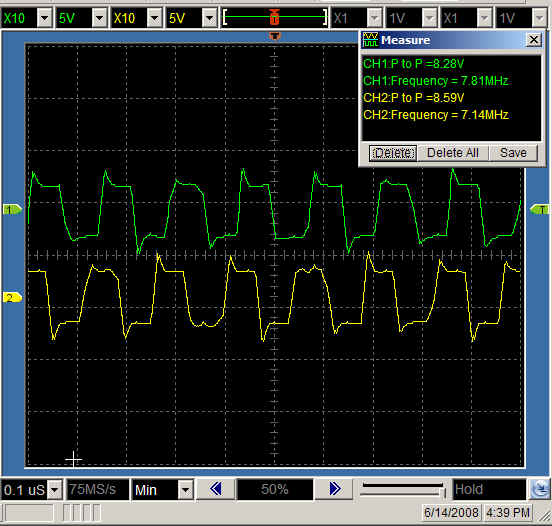
Testpoints D and E – FLO/4
Next, we see the result of the second division where the 2 signals of 14.112 MHz are reduced to 7.056 MHz and phase-shifted to put them into quadrature. Again, the values are approximations, given the limited capability of the PC USB Scope.
Completed Stage
Your radio now has the frequency determining capabilities necessary to drive and clock the Mixer stage. The next stage to be completed is, however, the Op-Amp stage. We will add the Op-Amp IC and its related components and then test it with audio signals (the same sort that will eventually come out of the Mixer stage).
Topside
Bottomside