Home BOM PS LO DIV Op-Amp RF Mixer Connect
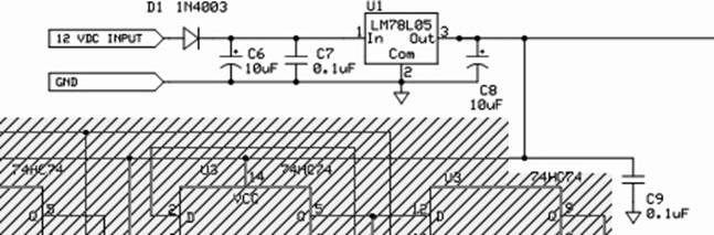
I - Softrock Lite V6.2 – Power Supply
Parts
|
Designation |
Description |
Type
Component |
Quantity |
|
D1 |
1N4003 Diode |
diode |
1 |
|
C6, C8 |
10uF Electrolytic |
Capacitor |
2 |
|
C7, C9 |
.01 uF SMT |
Capacitor |
2 |
|
misc |
9 volt |
|
1 |
|
misc |
power lead |
for 9 volt battery |
1 |
|
U1 |
LM78L05 (in IC bag) |
5 V Voltage Regulator |
1 |
Schematic
Installation Notes
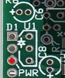
c Mount diode D1 (1N4003) in hairpin fashion, with the anode end flush with the round, lower hole and the band (cathode) end bent into a hairpin inserted into the hole in the square pad. This provides a good measuring point to validate the voltage across C6.

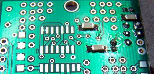
c U1 is a 5 volt regulator that will convert the 9-12 vdc input to a well-regulated voltage between 4.6 and 5.4 volts. Mount the U1 on the place provided, paying attention to the silk-screened pattern on the board.The three-hole patterns for mounting U1 are closely spaced and careful soldering is necessary to prevent solder bridges between leads and to make sure each lead is properly soldered.
c Using a length of lead that you have cut off after mounting D1, fashion a loop to serve as a ground test point and solder it into the two holes at the lower left hand corner of the board, bridging the two holes.
Electrolytic Capacitors
Pay careful attention to the polarity of electrolytic
caps. Note that the positive lead on an
electrolytic capacitor is the longer lead and goes into the hole marked
“+”. The shorter, negative lead is on
the side that has a grey band painted from the bottom to the top of the
cylinder. Slightly spread the leads of the capacitor
on the bottom side of the board to hold it in place and solder one lead. Check that the capacitor has been lightly
snugged to the board and reheat the solder if necessary to adjust the
position of the capacitor. Solder the second lead and cut both leads
flush to the bottom of the board.
c C6 10 uF electrolytic
c
C8 10 uF electrolytic
SMT Capacitors
Two SMT capacitors are mounted on the bottom side of the board in the locations shown below (see the video on SMT chip soldering)
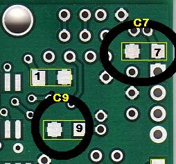
c C7 0.11 uF SMT
c C9 0.11 uF SMT
Tests
Connect the leads to the power pads (on the left side of the board, just to the southwest of U1 – see board layout above).
12 Vdc Power – Resistance Measurement
Before applying power, check the resistance on the two power terminals (PWR). The top hole is the positive and the hole below it is the negative/ground terminal. The resistance should be very high, on the order of 100K or better and will increase into the megohm range as the electrolytics charge up.
If you do not see the expected resistance, check the board for solder bridges or shorts.
Current draw
Note: Most of the stages will have a current draw test section. The author used a 9 V battery for all section current tests. One thing to note is that the current draw measurements will vary, depending upon the condition/freshness of the battery. If it is a weaker battery, you will see slightly higher values for the current draw.
For initial testing, connect the positive terminal of the battery via a 1K ohm current-limiting resistor in series with the positive lead and then connect your ammeter in series with the lead.
Once you have determined that the power connection is not fatally shorted, you can then remove the resistor and reconnect the meter in series with the power leads to measure the current draw.
c Expected current draw will be on the order of 3.8 to 4.0 mA, using a 9V battery as the power source.
c Actual measurement (author’s was 3.97 mA):_____________________
Voltage
Remove the ammeter from the power leads .
![]() Remember
to set the meter to Volts in the range that covers 5 volts.
Remember
to set the meter to Volts in the range that covers 5 volts.
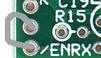
Place the negative probe on the negative power pad and the positive probe on the via that is just below C13 on the top of the board. See the graphic below:
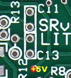
c You should measure a positive voltage between 4.6 and 5.4 Vdc.
c Actual measurement (author’s was 4.92 Vdc):__________________________
Completed Stage
You have completed stage I at this point and the board is getting the required power on the 5 Vdc rail. You are ready to move on to the next stage, the Local Oscillator. This next stage is the largest stage in terms of components that must be stuffed to the board. It will provide the 28.244 MHz signal that will subsequently be divided and shifted into the quadrature “L.O.” signals.
Top
Bottom