Softrock Lite II 03_Divider
Divider Introduction
General
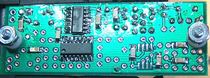
This stage will actually involve installing the remainder of the bottom-side components. In addition to installing all of the remaining SMT capacitors, you will also install the Mixer IC (U3), as well as the Divider IC (U2).
.Normally, the Mixer chip (U3) would be addressed in a separate "Mixer" Stage. However, due to the close proximity of the pads for the two Ics, U2 and U3, you will install it in this "Dividers" Stage.
The tests for U3 will be postponed until the "Mixer" Stage.
.Theory of Operation
The dividers accept as input the output of the local oscillator and divide that down to two signals that are ¼ the input frequency and in quadrature (90 ° out of phase with each other).
U2 is wired as a divide-by-4 synchroneous divider, clocked by the output from the Local Oscillator. Synchroneous clocking means that all stages switch at the same time, potentially offering a reduction of noise generated during switching.
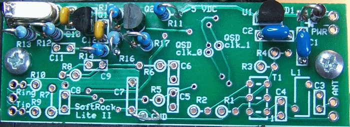
The divider provides two LO outputs which clock Mixer, U3. Proper Operation of the Dividers may be monitored on a CW or SSB receiver tuned to Divider Output Frequency listed in the table below.
| Band | Divider Output Freq |
|---|---|
| 160m | 1.843 MHz |
| 80m | 3.525 MHz |
| 40m | 7.056 MHz |
| 30m | 3.375 MHz |
| 20m | 4.6825 MHz |
| 15m | 7.015 MHz |
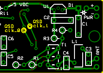
Note 1: A beat note should be heard when the antenna lead connected to a CW or SSB Receiver - tuned to Divider Output Frequency, is held near U2 on the SR Lite II PCB.
Note 2: All frequencies may be slightly below those stated in the table because of the loading capacitance is a little higher than specified for the nominal frequency of the Crystals supplied.
Divider Schematic
(Resistor testpoints (hairpin, top, or left-hand lead) are marked with red dots)
(Click for Full Schematic)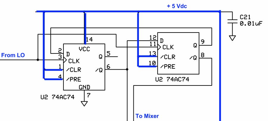
(above schematic has clickable areas that can be used for navigation)
Divider Bill of Materials
Detailed Bill of Materials
| Check | Designation | Component | Marking | Category | Orientation | Notes | Circuit |
|---|---|---|---|---|---|---|---|
| [____ ] | C14 | 0.01 uF |
 | SMT 1206 | Divider | ||
| [____ ] | C15 | 0.01 uF |
| SMT 1206 | Divider | ||
| [____ ] | C16 | 0.1 uF | black stripe
 | SMT 1206 | Divider | ||
| [____ ] | C17 | 0.1 uF | black stripe
| SMT 1206 | Divider | ||
| [____ ] | C18 | 0.1 uF | black stripe
| SMT 1206 | Divider | ||
| [____ ] | C19 | 0.1 uF | black stripe
| SMT 1206 | Divider | ||
| [____ ] | C21 | 0.01 uF |
| SMT 1206 | Divider | ||
| [____ ] | hdw1 | #4-40 board mounting hdw | HDW | Divider | |||
| [____ ] | hdw2 | #4-40 board mounting hdw | HDW | Divider | |||
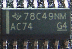
| [____ ] | U2 | 74AC74 Dual D FF | 74AC74
 | SOIC-14 | Divider | ||
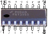
| [____ ] | U3 | FST3253 mux/demux switch | FST3253
 | SOIC-16 | Divider |
Divider Summary Build Notes
- Install remainder of the SMT Capacitors
- Install U3
- Install U2
- Install Hardware
- Test the Stage
Divider Detailed Build Notes
Bottom of the Board
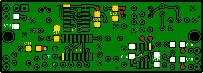
Install remainder of the SMT Capacitors
We will use this stage to go ahead and install all of the remaining SMT bypass capacitors.
The pads for the 0.1 uF capacitors are highlighted in white on the board shown above. These capacitors are in carrier strips marked with a black stripe.
The yellow markings pertain to the 0.01 uF capacitors.
Be very careful when soldering the following components, so as to avoid solder "splashover" that could clog the thru-holes for components installed latyer on in the project. The holes that are "at risk" are marked with a red dot on the above graphic. You might want to plug them up temporaily with a fine-pointed toothpick when soldering in their vicinity
- C14
- C18
- C19
- C20
- C21
- U4
| Check | Designation | Component | Marking | Category | Orientation | Notes |
|---|---|---|---|---|---|---|
| [____ ] | C14 | 0.01 uF |
| SMT 1206 | ||
| [____ ] | C21 | 0.01 uF |
| SMT 1206 | ||
| [____ ] | C15 | 0.01 uF |
| SMT 1206 | ||
| [____ ] | C16 | 0.1 uF | black stripe
| SMT 1206 | ||
| [____ ] | C17 | 0.1 uF | black stripe
| SMT 1206 | ||
| [____ ] | C18 | 0.1 uF | black stripe
| SMT 1206 | ||
| [____ ] | C19 | 0.1 uF | black stripe
| SMT 1206 |
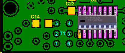
Install U3
You should install U3 BEFORE installing U2, due to layout considerations which could complicate the soldering of the Ics. The mixer will be tested in a later stage.
| Check | Designation | Component | Marking | Category | Orientation | Notes |
|---|---|---|---|---|---|---|
| [____ ] | U3 | FST3253 mux/demux switch | FST3253
| SOIC-16 | Take ESD precautions |
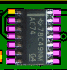
Install U2
Install 74HC74 (U2) on the SOIC-14 pads on the bottom side of the board. Take ESD precautions
| Check | Designation | Component | Marking | Category | Orientation | Notes |
|---|---|---|---|---|---|---|
| [____ ] | U2 | 74AC74 Dual D FF | 74AC74
| SOIC-14 | Take ESD precautions |
Top of the Board
Install Hardware
At this point you may install the two mounting screws and their associated hardware.
Install them with the screw head on the topside, then the board, then the spacer, then the washer, and finally the nut.
| Check | Designation | Component | Marking | Category | Orientation | Notes |
|---|---|---|---|---|---|---|
| [____ ] | hdw1 | #4-40 board mounting hdw | HDW | |||
| [____ ] | hdw2 | #4-40 board mounting hdw | HDW |
Divider Completed Stage
Top of the Board
Bottom of the Board
Divider Testing
Visual Check
Test Setup
Using very good lighting and magnification, carefully inspect the solder joints to identify bridges, cold joints, or poor contacts.
Pay especial attention to the joints on the divider IC pins. If necessary, touch up the joints with your iron and/or some flux. Wick up any excess.
Current Draw
Test Setup
- connect a 100 ohm resistor in series with the positive power lead
- apply 12 Vdc and measure the current draw with the limiting resistor in place
- remove the current limiting resistor
- apply 12 Vdc and measure the current draw without the limiting resistor
Test Measurements
| Testpoint | Units | Nominal Value | Author's | Yours |
|---|---|---|---|---|
| With the 100 ohm current-limiting resistor | mA | < 5 | 2.6 | _______ |
| Without the limiting resistor | mA | < 3 | 2.7 | _______ |
Voltage Tests
Test Setup
Measure the voltages with respect to ground for each of the pins of U2. Take care to measure at the actual IC pin rather than the pad, so as to ensure you are measuring the PIN voltage
expected voltages are indicated in the table below:
- 5 V (range of 4.5 - 5.4)
- 2.5 V (approx 50% of the 5V rail value)

Test Measurements
| Testpoint | Units | Nominal Value | Author's | Yours |
|---|---|---|---|---|
| Pin 1 | Vdc | 5 | 4.9 | _______ |
| Pin 2 | Vdc | 2.5 | 2.48 | _______ |
| Pin 3 | Vdc | 3.5 - 4.5 | 4.1 | _______ |
| Pin 4 | Vdc | 5 | 4.9 | _______ |
| Pin 6 | Vdc | 2.5 | 2.47 | _______ |
| Pin 7 | Vdc | 0 | 0 | _______ |
| Pin 8 | Vdc | 2.5 | 2.48 | _______ |
| Pin 9 | Vdc | 2.5 | 2.48 | _______ |
| Pin 10 | Vdc | 5 | 4.9 | _______ |
| Pin 11 | Vdc | 3.5 - 4.5 | 4.1 | _______ |
| Pin 12 | Vdc | 2.5 | 2.47 | _______ |
| Pin 13 | Vdc | 5 | 4.9 | _______ |
| Pin 14 | Vdc | 5 | 4.9 | _______ |
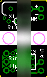
Divider Output
Test Setup
- The divider provides the QSD clocking signals for the mixer stage, with the frequency determined by the band for your kit. The bands and their QSD clocking frequencies are:
- 160m: 1.8432 MHz
- 80m: 3.515 MHz
- 40m: 7.056 MHz
- 30m: 10.125 MHz
- 20m: 14.0475 MHz
- 15m: 21.045 MHz
- The divider divides the LO frequency by 4, producing 2 frequencies that are at ¼ of the LO frequency and are 90° out of phase with each other.
- Using a ham receiver, dial up the QSD clocking frequency for the band in question and couple a wire from its antenna to point "QSD Clk 1" and then point "QSD Clk2" on the graphic below. You should hear the signal in the receiver.