Introduction
Theory of Operation
This stage provides the control interface between the hardware SDR and a PC that is running the appropriate SDR software which can provide I2C (Inter Integrated Circuit) bidirectional control signals over a USB connection. There are two lines in the I2C bus: the clock (SCL) and the date (SDA). For a more in-depth discussion of the I2C protocol, see the formal Specification.
The heart of the control circuit is U3, an ATTiny45-20PU 8 bit AVR Microcontroller (caution! the pdf for this device is over 4MB). The unit is powered off of the PC's USB 5 Vdc bus and provides a 6 bit bi-directional I/O port. It draws less than 10mA. The zener diodes in the schematic help ensure that the USB data lines (D+ and D-) are at 3.3V only.
U3 uses the AVR firmware by DG8SAQ to perform the following functions:
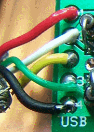
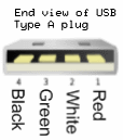
- Accept control signals via the pins 2 and 3 of the Universal Serial Bus (USB)
- Translate input signals into I2C control signals (bi-directional SDA and input-only SCL lines) for the Si570 programmable Oscillator
- Translate output I2C signals from the Si570 back to USB signals to the PC
- Translate incoming bandswitching commands into appropriate signals to J3 (for control of the new HF-BPF board.
- Future: new firmware for U3 is being developed to implement automatic band switching of the new HF-BPF switchable BPF.
Update
Several builders have experienced issues with the voltages on the USB-2 and USB-3 lines and diodes D2 and D3. Following a long series of messages on the Softrock Yahoo Group, Jan G0BBL and Tony KB9YIG have decided to address the issue as follows:
- Each new kit will be packed with two each of the BZY55 3.3 volt and 3.6 volt zener diodes in place of the two 1N5227B zener diodes for the D2 and D3 locations.
- Builders are advised to try the 3.6 volts BZY55 zener pair for D2 and D3 first, (marked on the glass body with 3V6), and if they still have USB communications reliability problems then go to the 3.3 volt BZY55 zener pair.
Schematic
This is a subset of the overall schematic. Note: red dot indicates resistor testpoints (hairpin, top, or left-hand lead)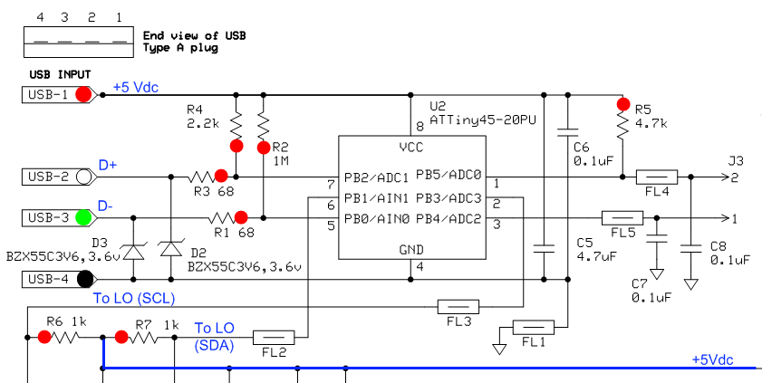
Bill of Materials
| Designation | Value | Color/Code | Orientation | Category | Notes |
|---|---|---|---|---|---|
| C06 | 0.1uF | SMT 1206 | black marked strip | ||
| C07 | 0.1uF | SMT 1206 | black marked strip | ||
| C08 | 0.1uF | SMT 1206 | black marked strip | ||
| FL1 | ferrite filter | SMT 1206 | |||
| FL2 | ferrite filter | SMT 1206 | |||
| FL3 | ferrite filter | SMT 1206 | |||
| FL4 | ferrite filter | SMT 1206 | |||
| FL5 | ferrite filter | SMT 1206 | |||
| D2 | 1N5227B,3.6v | N-S | do not use | ||
| D3 | 1N5227B,3.6v | S-N | do not use | ||
| D2 | BZY55,3.3v | N-S | See "Update" note in Introduction Section, above. | ||
| D3 | BZY55,3.3v | S-N | See "Update" note in Introduction Section, above. | ||
| D2 | BZY55,3.6v | N-S | Use this. See "Update" note in Introduction Section, above. | ||
| D3 | BZY55,3.6v | S-N | Use this. See "Update" note in Introduction Section, above. | ||
| C05 | 4.7uF | 475 | ceramic | ||
| R01 | 68 1/6W |
 | S-N | ||
| R03 | 68 1/6W |  | S-N | ||
| R05 | 4.7k 1/6W |

| E-W | ||
| R02 | 1M 1/6W |  | S-N | ||
| R04 | 2.2k 1/6W |  | S-N | ||
| R06 | 1k |  | S-N | ||
| R07 | 1k |  | S-N | ||
| U2 | ATTiny45-20PU | 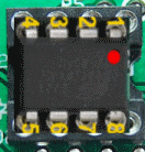 | with socket | ||
| J3 | 2 pin header | ||||
| cable1 | USB | 4 wire shielded USB cable with USB male on 1 end |
Summary Build Notes
- Install Zener diodes D2 and D3 (top)
- Install resistors and C5 ceramic cap (top)
- Install U2 and socket (top)
- Install J3 (top)
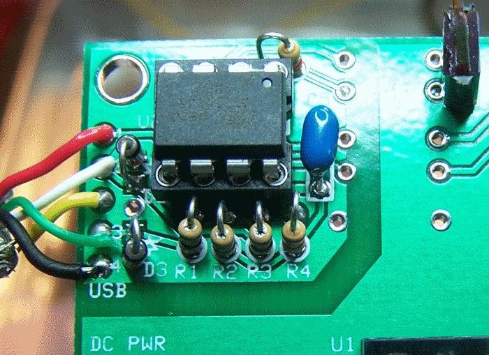
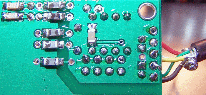
- Install and connect USB cable (top)
- Test the Stage
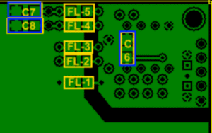
- Install SMT capacitors and ferrite filters (bottom)
Detailed Build Notes
In other stages, we prefer to begin with the bottom side of the board. However, in this stage, the thru-holes for the topside coponents are very close together and are just begging to get solder splashed into them if we were to install the SMT components first. Thus, in this stage, we have reversed the bottom-then-top sequence.
Top of the Board

Install Zener Diodes
Several builders have experienced issues with the voltages on the USB-2 and USB-3 lines. Jan G0BBL and Tony KB9YIG have decided to address the issue as follows:
- Each new kit will be packed with two each of the BZY55 3.3 volt and 3.6 volt zener diodes in place of the two 1N5227B zener diodes for the D2 and D3 locations.
- Builders are advised to try the 3.6 volts BZY55 zener pair for D2 and D3 first, (marked on the glass body with 3V6), and if they still have USB communications reliability problems then go to the 3.3 volt BZY55 zener pair.
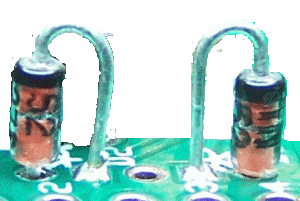
The two zener diodes are mounted hairpin style, with the cathode (banded) lead forming the hairpin.
| Designation | Value | Color/Code | Orientation | Category | Notes |
|---|---|---|---|---|---|
| D2 | BZY55,3.6v | N-S | Use this. See "Update" note in Introduction Section, above. | ||
| D3 | BZY55,3.6v | S-N | Use this. See "Update" note in Introduction Section, above. |
Install Resistors and ceramic capacitor C5
Note: 1/6W resistors are used due to the tight spacing of the resistors on the board.| Designation | Value | Color/Code | Orientation | Category | Notes |
|---|---|---|---|---|---|
| C05 | 4.7uF | 475 | ceramic | ||
| R01 | 68 1/6W |
 | S-N | ||
| R02 | 1M 1/6W |  | S-N | ||
| R03 | 68 1/6W |  | S-N | ||
| R04 | 2.2k 1/6W |  | S-N | ||
| R05 | 4.7k 1/6W |

| E-W | ||
| R06 | 1k |  | S-N | ||
| R07 | 1k |  | S-N |
Install U2 Socket
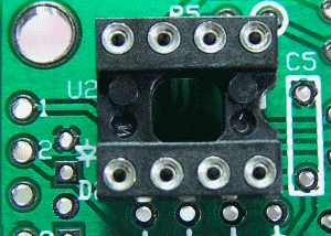
Install the socket for U2. Note the orientation on the notch, which should face eastward on the board
Install J3
J3 is reserved for a future use to provide control signals to the new HF_BPF (electronically switched bandpass fiters) kit.| Designation | Value | Color/Code | Orientation | Category | Notes |
|---|---|---|---|---|---|
| J3 | 2 pin header |
