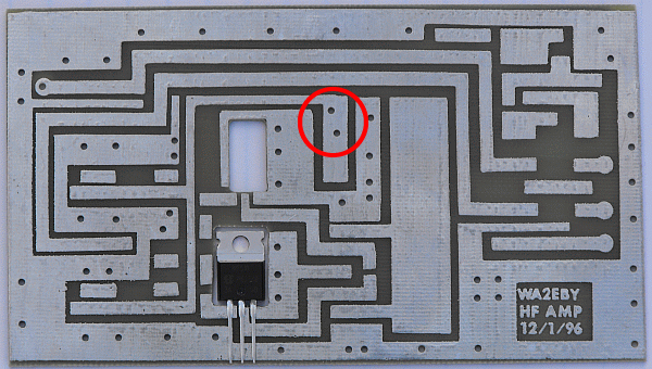
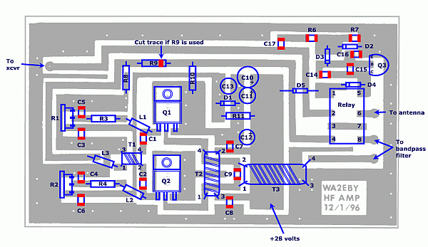
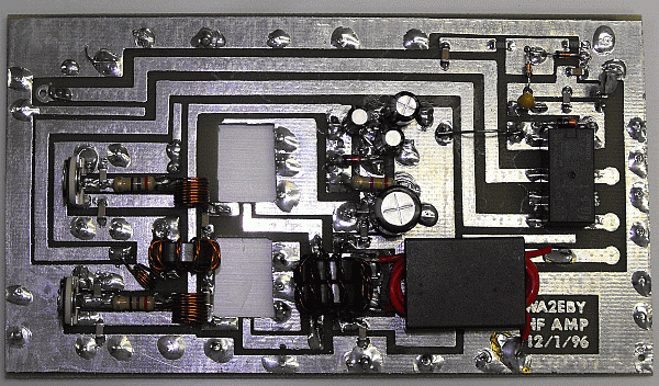
Important Error correction!
Do not install the shorting pins shown in the circle! If installed, they will short out the FET bias and you will be unable to bias the FET's on!
The FET's will not fit into the cutouts on the board as furnished. The cutouts need to be enlarged.
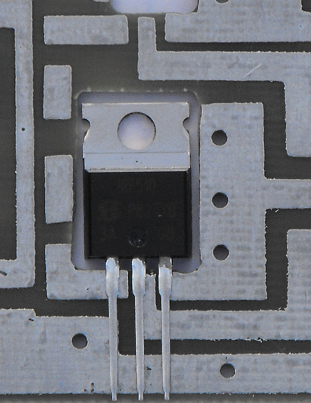
Using the FET leads and their final position as a guide, remove enough board material to allow easy insertion of the FET. In this picture, a little more material could be removed from the right. Do not cut into the 3 holes though. Those will be ground connections to the back of the board.
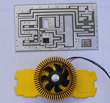
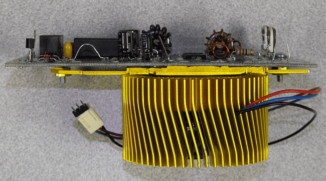
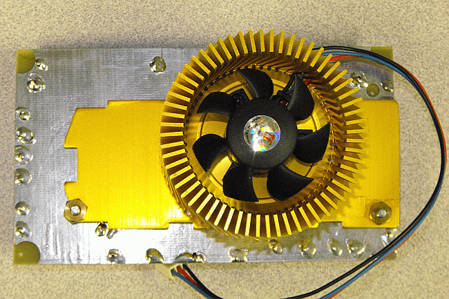
Selection of a heat sink will determine the allowable output power of the amplifier. I had a surplus computer heat sink and will use it. Most microprocessor's generate a lot of heat so a large computer heat sink should work well for us and are inexpensive and easily obtainable. If it isn't robust enough, it's easy to change out later. When testing the amplifier, I will monitor the output FET's temperature.
The FET's will attach to the heat sink using mica insulators and insulated hardware. After the board is assembled, we will drill and tap holes into the heat sink to screw the FET's down.
The holes for the connection of the ground plane on the opposite side of the board need to be soldered next. This connects the grounds on both sides of the board as the Far Circuits board does not have plated through holes. This can be done with wire in a similar fashion as done on the filter board or by using "pins" designed for the purpose. I had some pins from a purchase 20 years ago but I don't know of a current source. These pins make quick work of the grounding.
After enlarging both holes, the next step is to install all chip components. It is best to install all components of the same value at once to keep from mixing up the values.
Install C1 - C8. These are .1ufd chip capacitors. Use the ground holes on the board as guides for placement of the capacitors. While we are in the area, install C9. It is 47pfd.
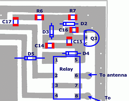
Next install C16 and C17. They are .001ufd.
C15. - .01ufd
R6 - 1k
R7 - 4.7k
That is the last of the chip components.
We will finish this section now.
Install:
D2 and D3 - 1N4148
If your relay coil voltage doesn't match the applied voltage, install D5 using a zener to reduce the voltage to your coil voltage.
Example:
Relay coil voltage is 12 volts, applied voltage is 24 volts, use a 12 volt zener.
C14 - 2.2ufd observing polarity. + side to the right.
D4 - 1N4004
Q3 - 2N3904
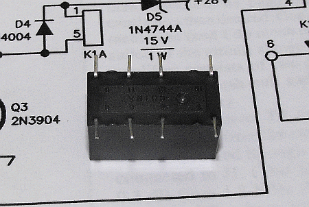
To mount the relay on the surface of the board, the leads will have to be bent outward from the body of the relay 90 degrees. This is easily done one side at a time by placing it on the edge of a table and while applying a little pressure, rotate the relay. This will do all 4 leads at once.
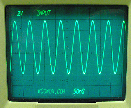
At this point, the rf switching circuitry is complete and you may test it.
The leads from the top are power and the 2 left leads are rf in. I used a signal generator set to 10MHz. It took a little over 5 volts pk-pk to make the relay switch. You should be able to hear it click.
Install the following components:
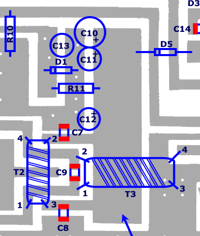
C10 - 100ufd 35 volts + side to the right
C13 - 15ufd 35 volts + side to the left
C11 - 15ufd 35 volts + side to the right
D1 - 5.1 volt zener cathode to the left
R11 - 2.4k 1/2 watt
C12 - 1ufd 35 volts + side to the right
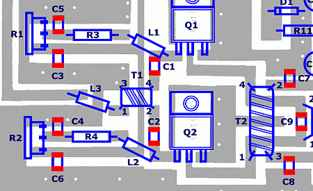
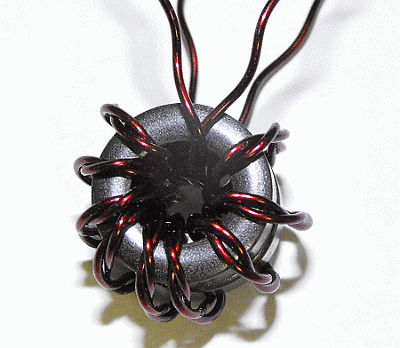
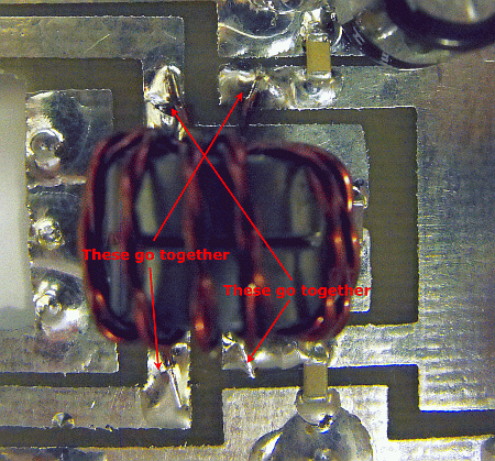
T2 will be 10 bifilar turns #22 on 2 stacked FT-50-43 cores. This will take about 38" of wire folded over in the middle and twisted.
T2 should look like this when wound. Tin them and meter them out to identify them.
Install T2 as shown. The 2 ends of the same wire are indicated on the picture.
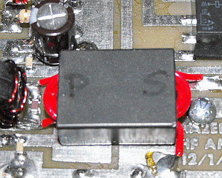
T3 uses a BN-43-3312 binocular core. The primary is 2 turns of #20 teflon insulated wire. It will take 8" of wire. The Secondary is 3 turns of the same wire. That will take 12" of wire. Install as shown below.
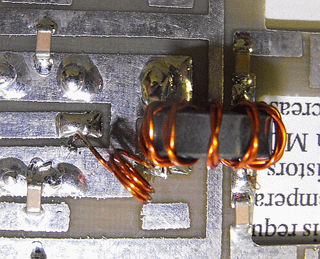
T1 is wound with 10 bifilar turns on #24 wire wound on a FT-50-43 core
Take 20" of #24 wire, fold it over in the middle and twist it about 5-8 turns per inch. After installation you should measure 0 ohms through the 2 left leads and 0 ohms through the 2 right leads.
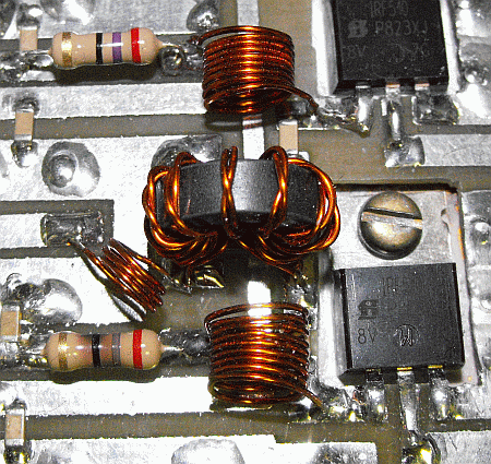
L3 is wound on a #12 or 3/16" drill shank. The shank end is the one you would put into the drill chuck. Wind 3 1/2 turns of #24 enameled wire close spaced. This will take about 3" of wire. Leave the newly wound coil on the drill shank while scrapping the enamel from the wire. The coil will retain it's shape better.
L1 and L2 are wound on a 1/4" drill shank using the same technique as L3 and with 9 1/2 turns of #24 enameled wire. Each coil will take 10" of wire. If you keep the wire close spaced while winding and under tension, it will retain it's shape better.
Install R3 and R4, 27 ohm, 1/2 watt before trying to solder the coils in. Otherwise, when soldering the resistors in, the coil wire may spring loose.
Final installation of T1 and the inductors should look as shown below. Your R4 doesn't have to be burned like mine. It survived a poorly planned test of the board.
Install R1 and R2, the FET's bias pots.
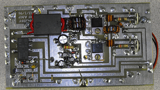
The board is now complete and ready for test.
When making RF measurements it is important to use both of the ground connections at the probes!
Install .001uf capacitors between the FET's gates and drains. These capacitors will connect the test signal from the gate to the drain of the FET's to allow signal phasing tests. They will be removed after the test and the FET's and the heatsink will be installed.
Connect a jumper wire between T3 pin 4 and K1 pin 8. This is where the bandpass filter connection will be made. This connects the output of T3 to the relay.
Connect power
Verify that the gate voltage is adjustable between 0 - 5 volts. Leave both pots set in the 0 volts position.
Connect a 10 volt pk-pk signal at a frequency between 2MHz and 30MHz. You should hear the relay click when applying the RF signal.
Connect your scope leads across the primary of T3 and trigger the scope on channel 1. This trigger setting is important to properly show the phase relationship between channel 1 and channel 2. Otherwise the scope will trigger at the same voltage and slope and will display the 2 waveforms in phase.
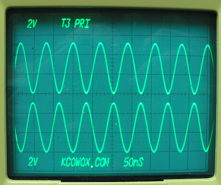
The waveforms should be 180 degrees out of phase and the same voltage.
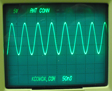
You should have approximately 17 volts out at the antenna connector.
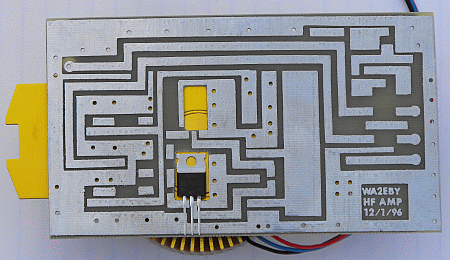
The board is now ready for installation of the heat sink.
Connect a 50 ohm load to the output connector. Apply power and measure the current. Adjust one of the bias pots for a 10ma increase and then adjust the other bias pot for an additional 10ma current draw. You should have approximately 30 ma's total draw with no RF input.