Building a Bitx20 Version 3
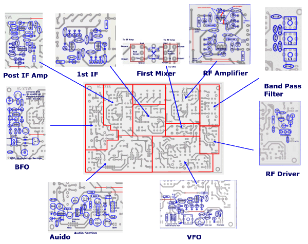
The board can be broken into sections and then built and tested one section at a time. This will make troubleshooting easier as any problems will be confined to one small section.
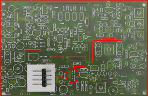
Install all of the wire jumpers onto the board. These can use bare or insulated wire. #22 wire will fit nicely through the holes. Place the jumpers where indicated by the red lines. If you have access to some header pins for the 4 pin power connector, it will make testing of the board a little easier as you can plug and unplug the wires between testing steps. We will be applying voltage to different pins of the 4 pin power connector to test the receiver and transmitter. This connector is to the right of the header pins and circled in the picture below. If you don't have the pins, a spdt switch or regular wires can be used.
Applying power to the R pin activates the receiver circuits. To the T pin activates the transmitter circuits. The V terminal activates the common circuits such as the BFO and the VFO. This will all be done automatically later by the PTT relay on the PA board.
When measuring current, place the + lead of the MA meter on the + terminal of the power supply and connect the - lead of the meter to the pin designated for power application called for by the instructions. This should be the R , T, or V pin of the power connector. The R and T pins should never be powered at the same time! The - lead of the power supply connects to ground on the board.
Band Pass Filter Section
For the band pass filter section you will need the following components.
|
Band pass Filter Components |
|||
|
quantity |
value |
description |
|
|
3 |
L1, L2, L3 |
provided with boards | |
|
2 |
0.1ufd |
capacitors | |
|
2 |
2.2pfd |
capacitors, npo | |
|
3 |
33pf or 47pfd |
capacitors, npo | |
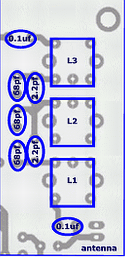
Using the parts placement diagram below, assemble the band pass filter section. Be very careful when inserting the transformers into the board. If the pins are misaligned, they will be pushed back into the can and are hard to retrieve. It is easiest to insert the 3 pin side first. Before you seat the can flush to the board, inspect the bottom side of the board and insure all pins are protruding. If a pin is pushed back, very carefully pull it back out with a pair of needle nose pliers.
After we assemble the next section, the RF amplifier, we can test it using a sweep generator. We will wait until then because it will provide the proper load impedance to the filter. If you don't have a sweep generator and oscilloscope, you can perform a basic alignment after the exciter is completed using an audio input and the exciter as an RF signal source. More on that procedure later.
RF Amplifier Section
For the RF amplifier section you will need the following components.
|
RF Amplifier Components |
||||
|
quantity |
value |
description |
color code |
|
|
2 |
10 ohm |
resistors | brn-blk-blk | |
|
2 |
100 ohm |
resistors | brn-blk-brn | |
|
4 |
220 ohm |
resistors | red-red-brn | |
|
2 |
1k |
resistors | brn-blk-red | |
|
2 |
2.2k |
resistors | red-red-red | |
|
8 |
.1uf |
capacitors | ||
|
2 |
1N4148 |
diodes | ||
|
1 |
2N3904 |
transistor | ||
|
1 |
2SC2570A |
furnished with boards | ||
Using the parts placement diagram below, assemble the RF amplifier section.
Note:
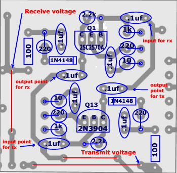
Install the transistors with the flat as shown on the drawing. The board silkscreen is not correct for 2N3904's. It is correct, however, for the 2SC2570A. Also, the 2SC2570A pins are not configured the same as the 2N3904's so is not directly interchangeable.
Note:
When setting the power supply voltage to measure the current, if you have 2 meters, hook one up as the ma meter and then meausre the voltage using the other where it enters the board. ma meters have an internal voltage drop and if you set the power supply to 13.25 volts, there will be less voltage at the board due to the meters voltage drop.
After assembly, apply 13.25 volts to the Receive voltage test point. The measured current should read approximately 11.7 ma's
Measure the Q1 voltages and compare to the chart below. There is space to document your readings after the standard voltages.
Disconnect the receive voltage line and connect the 13.25 volts to the Transmit voltage point. Warning! Do not ever have voltage applied to the Receive and Transmit point simultaneously! The measured current should read approximately 11.9 ma's .
ma's |
Measure the Q13 voltages and compare to the chart below.
|
Transistor voltages with 13.25 volts applied |
|||||
|
Receive - Q1 voltages |
Transmit - Q13 voltages |
||||
|
Collector |
8.76 |
Emitter |
2.008 |
||
|
Emitter |
1.995 |
Base |
2.703 |
||
|
Base |
2.711 |
Collector |
8.69 |
||
VFO Section
For the VFO section you will need the following components.
|
VFO Components |
||||
|
quantity |
value |
description |
color code |
|
|
1 |
10 ohm |
resistor | brn-blk-blk | |
|
3 |
100 ohm |
resistors | brn-blk-brn | |
|
4 |
1k |
resistors | brn-blk-red | |
|
1 |
2.2k |
resistor | red-red-red | |
|
1 |
4.7k |
resistor | yel-vio-red | |
|
2 |
10k |
resistor | brn-blk-orn | |
|
1 |
220k |
resistor | red-red-yellow | |
|
1 |
10pf npo |
capacitor | ||
|
1 |
220pf npo |
capacitor | ||
|
2 |
560pf npo/polystyrene |
capacitor | ||
|
5 |
.1uf |
capacitors | ||
|
1 |
6.5-30pf |
variable capacitor | ||
|
3 |
2N3904 |
transistor | ||
|
1 |
1N5239A or equiv 9.1 volt |
zener diode | ||
|
1 |
1N4752A or equiv 33 volt |
zener diode | ||
|
1 |
T37-6 with 50 turns #34 - 7.5 uh |
toroid coil | ||
Using the parts placement diagram below, assemble the VFO section.
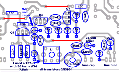
After assembly, apply 13.25 volts to the Voltage test point. The measured current should read approximately 44.8 ma's
ma's |
Measure Q5, and Q6 voltages and compare to the chart below. Your voltages may be slightly higher as my 9.1 volt zener is only 8.48. You can't measure the Q7 voltages until T1 is installed.
| Transistor voltages with 13.25 volts applied | ||||
|
Q5 |
Q6 |
|||
| Emitter |
3.56
|
2.84
|
||
| Base |
4.23
|
3.52
|
||
| Collector |
8.48 |
8.48 |
||
Mixer Section
For the mixer section, you will need the following components.
|
Mixer Components |
|||
|
quantity |
value |
description |
|
|
4 |
1N4148 |
diode | |
|
3
|
FT37-43 cores or supplied binocular cores |
T1, T1a, and T2 | |
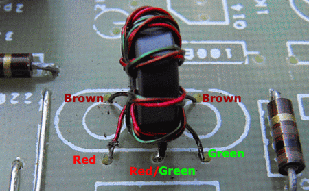
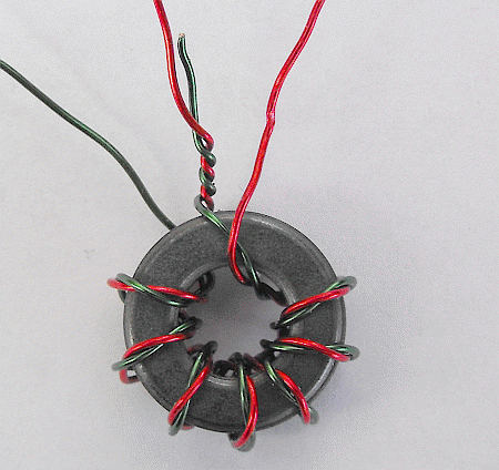
First we need to wind the trifilar transformers. You will need 2 for the mixer circuit and 1 more for the BFO so you might as well make all 3 now as they are all the same. All 3 will be on FT37-43 cores with 8 turns trifilar windings using #26 - #30 wire. You can find a video on winding trifilar transformers at
The transformers may be wound using either the supplied binocular cores or FT37-43 cores. You can investigate further by reading Wide-Band Transformers In the Bitx Instructions are included for both.
Use FT37-43 cores with 8 turns of trifilar wire. This will take 7" of trifilar wire for each transformer. 1 turn is 1 pass thru the center. We need 3 transformers total. 2 for the mixer and 1 for the BFO. I used red, green, and brown #28 wire but anything from #26 - #30 should be fine as size doesn't make much difference as long as it will fit into the core. The different colors make keeping the windings straight easier. When pulling the wire through the holes in the cores, be careful not to scrape the insulation off.
\![]() .
.
When you are through winding, it should look like this. Use the red wire from the right side of the picture and take the green wire from the left side of the picture and twist them together. This forms the center-tapped windings. If your wire is not heat strippable, strip of the insulation before twisting them together.
![]()
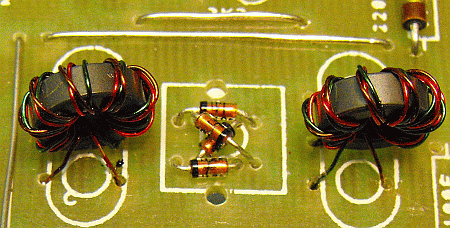
After tiinning, it should look like this. Install both transformers. Do not install the diodes yet.
Installed, T1 should look like this.
Using the supplied binocular cores
Use the binocular cores and wind 8 turns of trifilar wire onto the cores. 1 turn is a trip through both holes ending up where you started. We need 2 transformers. I had red, green, and brown #28 wire. The original drawing called for #32 but the size doesn't make much difference as long as it will fit into the core. The different colors make keeping the windings straight easier. When pulling the wire through the holes in the cores, be careful not to scrape the insulation off. The binocular cores can have sharp edges. When you are done, it should look like this.
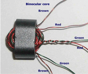
The completed transformer should look like this. Yours won't look so full as this one actually had 13 turns from and earlier build. Use 8 turns only though.
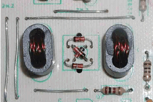
The installed binocular transformers should look like this. Do not install the diodes yet. Wait untill after you have performed the test below.
After winding and installing both transformers, verify continuity using an ohmmeter. There should be 0 ohms between the following points for both T1 and T1a. This step insures that the insulation was removed properly and you have good solder connections. Failure to completely remove the insulation may result in a faulty solder joint. This is a common failure item.
|
brown |
brown |
0 ohms |
|
|
green |
red-green or center tap |
0 ohms |
|
|
red-green or center tap |
red |
0 ohms |
Now we can measure the Q7 voltages. Apply 13.25 volts to the Voltage test point. The measured current should read approximately 84 ma's
ma's |
|
Q7 |
||
|
3.71 |
||
|
4.40 |
||
|
8.85 |
||
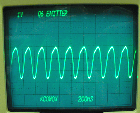
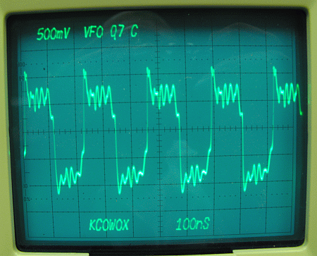
If you have an oscilloscope, using a x10 probe, connect to the collector of Q7.
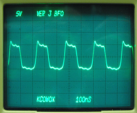
The frequency should be variable using the tuning capacitor. I have a 10-365pfd variable and the frequency will vary from 3.8mhz to 4.8mhz. We will trim the frequency to the proper range later.
Using the parts placement diagram below, install the 4 diodes observing the proper polarity. The band is the cathode end.
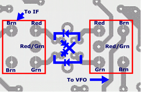
Bend the leads and position them observing the black bands as shown below.
Q7 collector waveform now is:
The signal is clipped to +/- about .7 volts as the diodes bias on. If the waveform wasn't clipped or only clipped on one side, the problem would be an open in the diode circuit or a bad diode.
1st IF Amplifier Section
This is almost an exact duplicate of the RF Amplifier section. For the 1st IF Amplifier section you will need the following components.
|
1st IF Amplifier Components |
||||
|
quantity |
value |
description |
color code |
|
|
2 |
10 ohm |
resistors | brn-blk-blk | |
|
2 |
100 ohm |
resistors | brn-blk-brn | |
|
4 |
220 ohm |
resistors | red-red-brn | |
|
2 |
1k |
resistors | brn-blk-red | |
|
2 |
2.2k |
resistors | red-red-red | |
|
8 |
.1uf |
capacitors | ||
|
2 |
1N4148 |
diodes | ||
|
2 |
2N3904 |
transistors | ||
Using the parts placement diagram below assemble the 1st IF amplifier section.
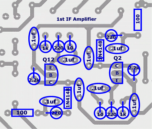
After assembly, apply 13.25 volts to the Receive voltage test point and the voltage test point. The measured current should read approximately 109.2 ma's
ma's |
Measure the Q2 voltages and compare to the chart below.
Disconnect the receive voltage line and connect the 13.25 volts to the Transmit voltage point.
Warning! Do not have voltage applied to the Receive and Transmit point simultaneously!
The measured current should read approximately 109.2 ma's
ma's |
Measure the Q13 voltages and compare to the chart below.
|
Transistor voltages with 13.25 volts applied |
|||||
|
Q2 voltages |
Q12 voltages |
||||
|
Collector |
8.74 |
Collector |
8.76 |
||
|
Base |
2..708 |
Base |
2.696 |
||
|
Emitter |
1.988 |
Emitter |
1.970 |
||
Q2 and Q12 circuits are identical so the differences in measured voltages are due to component tolerances.
2nd IF Amplifier
We are going to skip the crystal filter for now. To check our crystals and match them we need an oscillator. We will have one after we complete the BFO section. Also, this is a good spot to leave open to allow easy testing with test equipment later.
We will need the following components for the 2nd IF Amplifier.
|
2nd IF Amplifier Components |
||||
|
quantity |
value |
description |
color code |
|
|
1 |
4.7 ohm |
resistor | yel-vio-gld | |
|
1 |
22 ohm |
resistor | red-red-blk | |
|
2 |
100 ohm |
resistors | brn-blk-brn | |
|
4 |
220 ohm |
resistors | red-red-brn | |
|
2 |
470 ohm |
resistor | yel-vio-brn | |
|
2 |
1k |
resistors | brn-blk-red | |
|
1 |
2.2k |
resistors | red-red-red | |
|
1 |
10k |
resistor | brn-blk-org | |
|
1 |
47k |
resistor | yel-vio-org | |
|
8 |
.1uf |
capacitors | ||
|
2 |
1N4148 |
diodes | ||
|
3 |
2N3904 |
transistors | ||
Using the parts placement diagram below assemble the 2nd IF amplifier section.
Note: The 4.7 ohm resistor in the drawing below is correct. The silkscreen on the board may show 10e. Use a 4.7 ohm here.
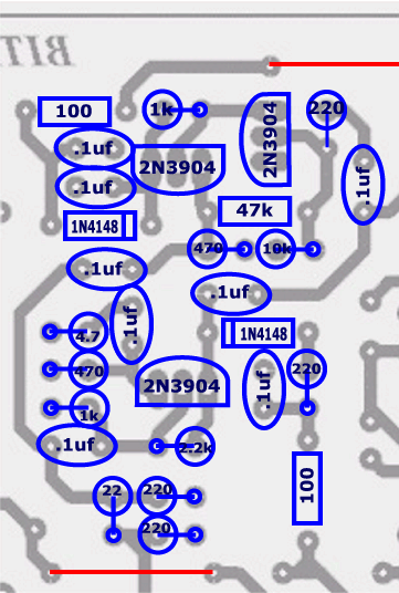
Apply 13.25 volts to the receive line and the voltage line.The measured current should be approximately 124.7 ma's.
ma's |
Measure and verify the voltages in the chart below for Q3 and Q3A.
|
Receive transistor voltages with 13.25 volts applied |
|||||
|
Q3 |
Q3A |
||||
|
Collector |
6.08 |
Collector |
10.78 |
||
|
Base |
.71 |
Base |
6.07 |
||
|
Emitter |
0 |
Emitter |
5.35 |
||
Remove the voltage from the receive line and apply it to the transmit line The measured current should be approximately 117 ma's. Measure and verify the voltages in the chart for Q11.
Transmit transistor voltages with 13.25 volts applied |
||
| Q11 | ||
| Collector | 9.90 | |
| Base | 3.118 | |
| Emitter | 2.405 | |
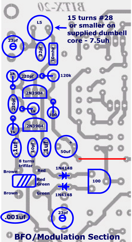
BFO Section
We will need the following components for the BFO section.
|
BFO Section Components |
||||
|
quantity |
value |
description |
||
|
1 |
100 ohm |
resistor | brn-blk-brn | |
|
3 |
1k |
resistors | brn-blk-red | |
|
1 |
120k |
resistor | brn-red-org | |
|
1 |
10pf |
capacitor - npo | ||
1 |
22pf |
capacitor - npo | ||
|
2 |
23pf |
variable capacitors | ||
|
2 |
220pf |
capacitor - npo | ||
1 |
.001uf |
capacitor | ||
|
2 |
.1uf |
capacitors | ||
|
1 |
50uf |
capacitor | ||
|
1 |
10 mhz |
crystal | ||
|
1 |
7.5uh |
inductor (see text) | L5 | |
|
1 |
100 ohm |
potentiometer | ||
|
1 |
T2 |
transformer (see text) | ||
|
2 |
1N4148 |
diodes | ||
|
2 |
2N3904 |
transistors | ||
2 |
socket pins |
|||
We wound T2 earlier in the mixer section. If you didn't at that time, refer back the the mixer section for directions.
Using the parts placement diagram below assemble the BFO section. If you can obtain 2 plug in socket pins for the crystal, we will use the bfo oscillator to help match the crystal filter crystals frequency before we build the crystal filter.
After assembly, apply 13.25 volts to the Voltage test point and ground to the ground point. We don't need any voltage on the Rx or Tx as the BFO runs all of the time.
The measured current should read approximately 98.6 ma's
ma's |
Measure Q8 and Q9 voltages and compare to the chart below.
|
Transistor voltages with 13.25 volts applied |
|||||
|
Q8 voltages |
Q9 voltages |
||||
|
Collector |
11.99 |
Collector |
11.99 |
||
|
Base |
6.41 |
Base |
6.30 |
||
|
Emitter |
6.32 |
Emitter |
5.81 |
||
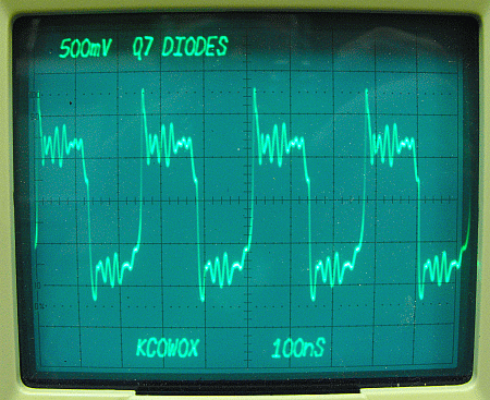
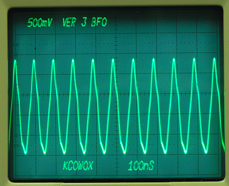
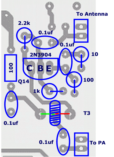
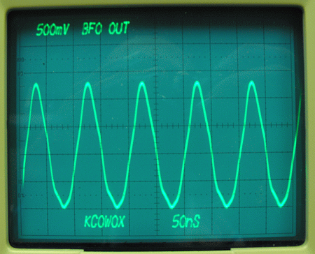
If you have an oscilloscope, connect as shown below to see the bfo output waveform.
You should see the waveform below.
If you have a frequency counter, an easy way to get the correct frequency range is a test hookup shown below. Using this method, wind a couple of extra windings on the dumbell core and install it using a test plug made from an cut up IC socket. This will prevent damaging the board with repeated soldering/desoldering operations. A good place to connect the counter is at the junction of T2 and the 0.1uf cap as shown in the picture above. Apply power and adjust the variable cap to the middle of it's range. Remove a turn or two until the frequency is near 9,995,268 hz. This should be close enough that it should adjust properly later.
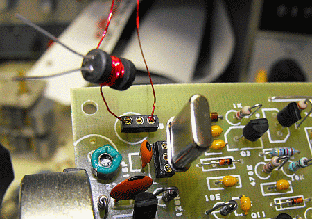
My BFO frequency, when adjusted properly for the filter on my board, was 9,995,268 hz.
If you don't have access to a counter, just wind the 15 turns on the core.
Audio Section
We will need the following components for the Audio Section.
|
Audio Section Components |
||||
|
quantity |
value |
description |
||
|
1 |
10 ohm |
resistor | brn-blk-blk | |
|
1 |
100 ohm |
resistor | brn-blk-brn | |
|
2 |
220 ohm |
resistors | red-red-brn | |
|
2 |
2.2k |
resistors | red-red-red | |
|
2 |
4.7k |
resistors | yel-vio-red | |
|
1 |
10k |
resistor | brn-blk-org | |
|
1 |
120k |
resistor | brn-red-yel | |
|
1 |
100pf |
capacitor | ||
|
2 |
.001uf |
capacitors | ||
|
2 |
.1uf |
capacitors | ||
|
4 |
1uf |
capacitors | ||
|
3 |
50uf |
capacitor | ||
|
2 |
220uf |
capacitors | ||
|
1 |
LM386 |
audio amp IC | ||
|
1 |
1N4148 |
diode | ||
|
2 |
2N3904 |
transistors | ||
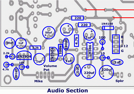
Using the parts placement diagram below assemble the audio amplifier section.
After assembly, apply 13.25 volts to the Voltage test point, the Rx test point, and ground to the ground point. Do not connect the volume control pot or the speaker. The measured current should read approximately 146 ma's
ma's |
Measure the Q4 voltages and compare to the chart below.
|
Transistor voltages with 13.25 volts applied |
|||||
|
Q4 voltages |
Q10 voltages |
||||
|
Collector |
2.234 |
Collector |
9.16 | ||
|
Base |
.709 |
Base |
4.18 | ||
|
Emitter |
0 |
Emitter |
3.50 | ||
Remove the voltage from the RX test point and apply it to the TX test point. Leave the voltage applied to the V test point and measure the Q10 voltages and compare to the chart above.
Crystal Filter
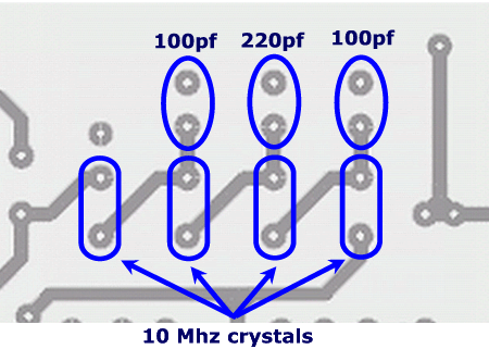
We will need the following components for the crystal filter.
|
Crystal Filter Components |
|||
|
quantity |
value |
description |
|
|
2 |
100pf |
capacitors | |
|
1 |
220pf |
capacitor | |
|
4 |
10 mhz |
crystals | |
If you have access to a frequency counter, the crystals should be matched as close as possible in frequency. This is done by inserting them into the BFO circuit and counting the frequency. This is best done using at least 10 crystals.
Assemble the crystal filter using the drawing below.
Output Driver
We will need the following components for the output driver.
|
Output Driver Components |
||||
|
quantity |
value |
description |
||
|
1 |
10 ohm |
resistor | brn-blk-blk | |
|
2 |
100 ohm |
resistors | brn-blk-brn | |
1 |
1k |
resistor | brn-blk-red | |
|
1 |
2.2k |
resistor | red-red-red | |
|
4 |
.1uf |
capacitors | ||
|
1 |
2N3904 |
transistor | ||
1 |
transformer |
FT37-43 | ||
The transformer may be made using a FT37-43 core. Wind 8 bifilar turns on the core . This will take 6" of wire. Take the left side red and the right side green and twist together to form the center tap.
Assemble the components as shown below.
After assembly, apply 13.25 volts to the Voltage test point the Tx test point, and ground to the ground point. The measured current should read approximately 159 ma's
ma's |
Measure the Q44 voltages and compare to the chart below.
| Q14 | ||
| Collector | 10.58 | |
| Base | 3.19 | |
| Emitter | 2.47 | |
Test and alignment
Connect the variable tuning capacitor to the board. Apply power to the voltage connection. Do not apply to the Rx or Tx connector.
The following readings will confirm operation of the BFO and the VFO.
Communications receiver method::
BFO
Move the wire nesr Q9 and Q9 and tune the receiver around 9.996 mhz. Verify that the signal you are receiving is your board by turning off the power to your board.
VFO
Move the wire near Q6 and Q7. Tune the receiver in the 4.150 to 4.350 range. Verify that the signal you are receiving is your board by turning off the power to your board.
Using a "Sharpie" RF probe or scope:
Using a "Sharpie" RF Probe as detailed at http://golddredgervideo.com/kc0wox/rfprobe.htm you should get the following readings. These readings will be very approximate as the RF Probe readings are more of a presence and magnitude reading.:
RF Probe
BFO junction of primary T2 and capacitor - .674 volts
Scope
RF Probe
VFO junction of Q6 emmiter and 1k resistor - 1 volt
Scope
RF Probe
VFO collector of Q7 - .59 volts.
Scope
Aligning the BFO
The proper BFO frequency will end up around 9.9953mhz.
Connect the frequency counter to the emitter of Q9. You should
have a tuning range of around 15khz. You can raise the frequency
by removing turns from L5. If your frequency is too high, you
can add capacitance in parallel with the trimmer capacitor. Once
you get the frequency close, verify it this way.
Connect your "sharpie" RF probe to the PA output
point.
Connect power to the transmit point.
Adjust the carrier balance pot to one end and note the reading.
Adjust it to the other end.
Set it to the end that gave the most voltage out.
Adjust the BFO frequency while watching the voltage reading until
a peak is reached.
At this point the BFO is adjusted to the top
of the lower skirt of the filter.
Note the reading and then adjust the BFO frequency back down until it reads about 0.45 of the maximum reading. This will set it about 7-8 db down the filter skirt.
This setting is as close as we can get until we add modulation.
Aligning the VFO
Connect the counter to the emitter of Q6. Verify the tuning
range of the VFO. If it is too low, remove turns from L4.
If it is too high, add capacitance in parallel with the 220pf
capacitor. If it has too wide a tuning range, add capacitance
in series with the variable tuning capacitor. Use only npo
capacitors or the VFO may drift excessively.
Aligning the Bandpass Filter
Adjust the VFO frequency to 4.250mhz.
The easiest way with no test equipment is while
in receive, connect an antenna to the RX Ant point and adjust
the filter transformers for maximum volume out. This is probably
the easiest way and can be refined later after the PA is connected.
Alternate way 1:
W
hile in transmit and monitoring the PA Output
voltage at the left hand side of the 0.1ufd that is connected
to T3, labeled "To PA" in the exciter schematic, with an
RF probe or oscilloscope, adjust the 3 transformers for the
maximum displayed voltage.
Alternate way 2:
Monitor the power supply current while
in transmit and adjust the transformers for maximum current.
If you can't see any variation, adjust the carrier balance
pot to one end. This will insert carrier and cause the output
voltage or the power supply current to increase.
Now readjust the carrier balance and the balance capacitor for minimum voltage reading. We will refine this setting after the linear is connected.
The alignment of the exciter is now done.